

Understanding semiconductor nanowire growth
Semiconductor nanowires are quintessential nanoscale building blocks and the vapor-liquid-solid technique – where a liquid “catalyst” droplet collects atoms from the vapor and directs crystallization of individual solid layers – is a workhorse method for their synthesis. The encoding of different functionalities (e.g., heterostructures, pn junctions, etc.) along the length of individual nanowires makes these materials interesting for a range of electronic, photonic, and energy applications.

Vapor-liquid-solid (VLS) nanowire synthesis and the functional encoding (left, doping; right, heterostructuring) possible by tuning gas phase composition.
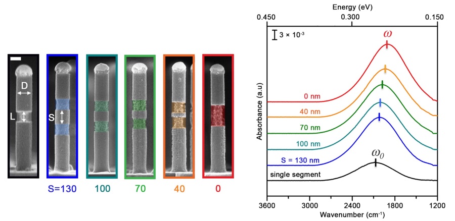
The inability to synthesize many desired, and even simple, nanowire structures demonstrates that the mechanistic understanding of growth is far from complete. We combine in situ infrared spectroscopy with electron microscopy to connect the specific, short-lived chemical bonds present during growth with nanowire crystal structure and physical properties. Our studies are providing an atomic-level chemical framework with which to understand nanowire growth and rationally tune the relative rates of important, structure-directing surface reactions.

Transient sidewall chemistry controls Ge nanowire growth stability (From: Sivaram et al, J. Am. Chem. Soc. 2015)
Engineering nanowire structure
We are leveraging our understanding of nanowire growth to design chemistries that endow nanowires with a structural precision and functional diversity superior to the state-of-the-art. Independent control of the chemical bonding at each of the heterointerfaces involved in vapor-liquid-solid growth is essential, but not possible with conventional 2-D thin film precursors (e.g., hydrides). Our approach utilizes multiple distinct precursors, each designed to direct a specific heterointerfacial process, to choreograph synthesis. This precursor "toolkit" allows us to engineer nanowire crystal orientation, bilayer stacking sequence, diameter, dopant profile, and more.

Kinking superstructures via precursor design (From: Musin et al, Nano Lett. 2012)
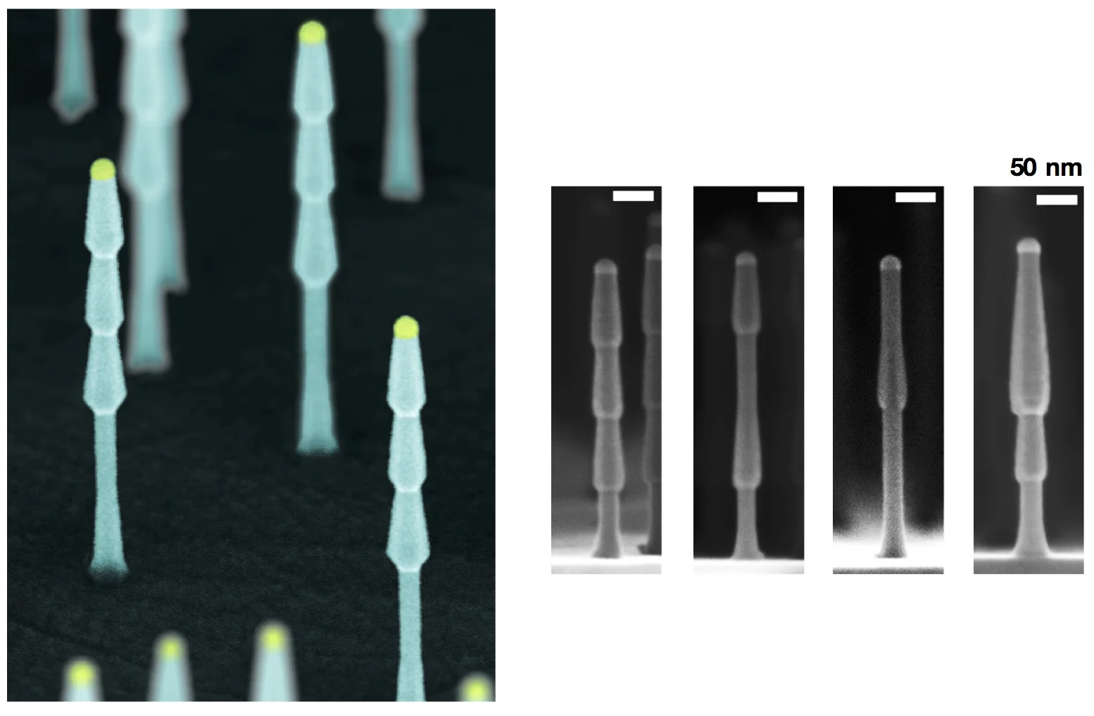
Surface passivation blocks sidewall deposition and permits programming of nanowire diameter (From: Musin et al, J. Vac. Sci. Technol. B 2013)
Semiconductor nanowire plasmonics
Surface plasmons enable the confinement and transport of light in deep-subwavelength volumes. Noble metals offer this extraordinary capability in the visible/near-infrared, yielding extreme chemical sensitivity (e.g., surface enhanced Raman scattering), high resolution near-field imaging, compact waveguides, and more. However, conventional metals cannot support truly localized surface plasmon resonances (LSPRs) at mid-/far-infrared wavelengths since they become nearly perfect conductors.
Nanoscale semiconductors are emerging as alternative, more flexible materials for manipulating light-matter interactions in the infrared. The tunability of semiconductor permittivity via chemical doping and/or electrostatic gating is central to their promise. Vapor-liquid-solid growth of semiconductor nanowires, which offers nanoscale control of dopant profile, provides an intriguing route to engineer both near- and far-field optical response. We are synthesizing and characterizing a range of plasmonic semiconductor nanowires with the goal of enabling narrowband infrared light sources, compact thermal waveguides, and ultrasensitive chemical sensors.
Using coupled localized surface plasmon resonances (LSPRs) in semiconductor nanowires to focus infrared light (From: Boyuk et al, ACS Photon. 2016)
Nanowire manufacturing
While semiconductor nanowires can be produced with exquisite control of composition and morphology using the vapor-liquid-solid mechanism, growth on flat substrates constrains production rates and limits the use of these materials to boutique applications. To overcome this challenge, we are developing new methods to scale-up the manufacturing of high quality nanowires and nanowire devices. The Geode process, for example, promises the synthesis of functionally-encoded semiconductor nanowires at throughputs orders of magnitude beyond the state-of-the art. Central to the Geode process are sacrificial, porous-walled, seed particle-lined silica microcapsules, whose interior surface serves as a high-surface area growth substrate. Microcapsules protect the growing nanostructures, are produced with a scalable emulsion templating technique, and are compatible with large-scale chemical reactors.

Hollow microcapsules provide a high surface for nanowire growth, efficient gas transport to enable compositional-encoding, and mechanical protection during processing.